Abstract
Free full text

A 512×512 SPAD Image Sensor with Integrated Gating for Widefield FLIM
Abstract
We report on SwissSPAD2, an image sensor with 512×512 photon-counting pixels, each comprising a single-photon avalanche diode (SPAD), a 1-bit memory, and a gating mechanism capable of turning the SPAD on and off, with a skew of 250ps and 344ps, respectively, for a minimum duration of 5.75ns. The sensor is designed to achieve a frame rate of up to 97,700 binary frames per second and sub-40ps gate shifts. By synchronizing it with a pulsed laser and using multiple successive overlapping gates, one can reconstruct a molecule’s fluorescent response with picosecond temporal resolution. Thanks to the sensor’s number of pixels (the largest to date) and the fully integrated gated operation, SwissSPAD2 enables widefield FLIM with an all-solid-state solution and at relatively high frame rates. This was demonstrated with preliminary results on organic dyes and semiconductor quantum dots using both decay fitting and phasor analysis. Furthermore, pixels with an exceptionally low dark count rate and high photon detection probability enable uniform and high quality imaging of biologically relevant fluorescent samples stained with multiple dyes. While future versions will feature the addition of microlenses and optimize firmware speed, our results open the way to low-cost alternatives to commercially available scientific time-resolved imagers.
I. Introduction
Fluorescence lifetime imaging microscopy (FLIM) is an important tool in life sciences, including biophysics and biochemistry. Major advantages of lifetime imaging over conventional fluorescence intensity imaging include insensitivity to fluorophore concentration [1], photo-bleaching, and depth [2, 3]. In addition, the sensitivity of fluorescence lifetime on various environmental parameters such as oxygen levels or pH makes it a useful tool in functional imaging. Finally, FLIM permits rejection of background fluorescence by gating, when background lifetime is significantly different from that of the target fluorophores [4].
Commonly used image sensor technologies for time-domain widefield FLIM consist in time-gated image intensifiers coupled with sCMOS or CCD cameras [5, 6], or microchannel plate (MCP) and photocathode-based widefield detectors [7]. Time-gated image intensifiers suffer from low dynamic range, due to the large gain of the intensifier, and are costly. MCPs are limited in the maximum achievable global count rate and are equally costly and complex to use due to the ultrahigh-voltages involved. The development of single-photon avalanche diodes (SPADs) in standard CMOS technologies [8], and the introduction of large CMOS SPAD arrays [9], has created a potential for multichannel single-photon counting with parallel readout and fast data processing. SPADs can reach high timing performance thanks to fully integrated gating options [10, 11, 12], and have no global count limitations, as CMOS technology supports modular, scalable building blocks with large counters and fast electronics. Until recently, the main obstacle towards megapixel time-resolved SPAD imagers was the miniaturization of a “smart” SPAD pixel that employs dedicated time-stamping and photon-counting circuits. In addition, high dark count rate (DCR) and low photon detection efficiency (PDE) made SPAD imagers less competitive compared to sCMOS and EMCCD sensors [13].
In this paper, we introduce SwissSPAD2, a SPAD imaging sensor comprising 512×512 pixels, the largest format to date, with time-resolved imaging capability based on time gating. SwissSPAD2 employs a p-i-n SPAD with one of the best PDP spectrum and DCR combinations among SPADs in standard processes [14]. We also present time gating characterization to evaluate the time-resolved imaging performance of SwissSPAD2. Finally we report on widefield FLIM tests performed with different fluorescent samples.
II. Image Sensor Architecture
A. p-i-n SPAD
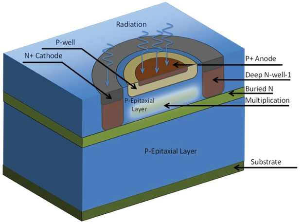
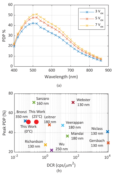
The SPAD used in this sensor is based on a p-i-n junction [14]. It was designed to achieve low DCR and crosstalk, at the expense of a relatively low fill factor. As shown in Fig. 1, a lightly doped p-epi guard ring layer around the p-well prevents premature edge breakdown (PEB), i.e. electron multiplication in the peripheral junctions resulting from an electric field exceeding the critical value for silicon. However, lower electric field in the outer parts of the pwell results in lower PDP in the junction periphery, which reduces the average PDP of the SPAD. The timing jitter of the SPAD varies between 97.2 ps and 139.5 ps, depending on wavelength and excess bias. Its PDP at 7 V excess bias reaches a maximum of 50% at 520 nm, and exceeds 30% across the visible spectrum (Fig. 2(a)) [15]. Its minimum (Vex= 3 V) dark count rate is 0.18 cps/μm2. All measurements in this paper obtained with SwissSPAD2 were performed at Vex = 3.5 V unless stated otherwise.
A comparison of published SPAD PDP and DCR is shown in Fig. 2(b). In the literature, among SPADs in standard processes only Bronzi [16] reports lower noise and higher peak PDP than those of SwissSPAD2; however, Bronzi’s SPAD features a much narrower PDP spectrum due to a shallower junction.
B. Pixel Circuit and Operation
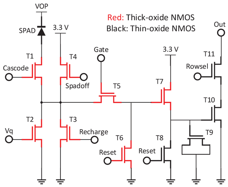
The p-i-n SPAD is embedded in a digital pixel with a total of 11 NMOS transistors. Shown in Fig. 3, the main functions of the pixel are: passive quenching (T2), active recharge (T3), time gating (T3, T4, T5), 1-bit DRAM (T9), memory reset (T7 and T8), and digital readout (T10) [18]. The cascode transistor (T1) is added to reliably increase the maximum excess bias from 3.6 V to 5.2 V, which is beyond the standard operating voltage of the employed CMOS technology [19]. The increase in the maximum excess bias from 3.6 V to 5.2 V results in approximately 20% PDP improvement, at the expense of approximately 65% increase in DCR at 25°C. The possibility to tune the excess bias provides a wide range of options in the trade-off between high PDP and low DCR. The basic operation of the pixel is illustrated in Fig. 4. The gating signals are sent to the pixel array independently from the readout signals. Consequently, time gating parameters such as timing resolution and measurement range do not affect the readout speed. The gate signals are synchronized with the laser clock. If the pixel detects a photon within the time-gate, the 1-bit DRAM is charged. The frame readout is performed in 10 μs in a rolling shutter mode (with global shutter exposure). Note that only one photon can be detected during the readout cycle (introducing count loss or pile-up, which can be corrected during post-processing [20]), although we use multiple gates per readout. Unlike charge accumulating CCD/CMOS and analog SPAD imagers [21], multiple photon counts cannot be stored in a single capacitor. In digital SPAD pixels, counters or multiple RAM modules are needed, which occupy large areas thus reducing fill factor if implemented at the pixel level. The choice of a 1-bit digital pixel maximizes fill factor and eliminates readout noise, leaving dark counts (and afterpulsing) as the only noise sources in the system. The choice of a 1-bit digital pixel is in this particular case also justified by the usually low photon count rates in lifetime imaging. This 11T pixel has a 16.38 μm pitch and a 10.5% fill factor. Microlenses are expected to improve the fill factor five-fold, to reach over 50%, based on design simulations and previous measurements [20].
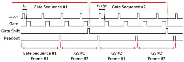
Timing diagram of the sensor in rolling shutter mode. The number of frames per gate sequence and the number of gate sequences are user-selectable parameters. In this figure, both parameters are set to 2 for simplicity. A higher number of 1-bit frames per gate sequence leads to higher dynamic range. The gate shifting process introduces a dead time of 65 ns per 35.7 ps shift, which is insignificant compared to the readout of a single frame.
The largest advantage of the SPAD technology, when compared to most other single-photon detectors, is the combination of picosecond-range temporal resolution and large spatial resolution. Therefore, the performance characteristics related to time-resolved widefield imaging are of high importance in SPAD sensors. The most accurate time-resolved detection is performed with a time-to-digital converter (TDC), which measures the delay between the emission of a laser pulse and its detection by the sensor. Unfortunately, TDCs are too bulky to be integrated in a compact monolithic pixel. The existing methods of TDC sharing by a group of pixels require the placement of the TDC inside the pixel array, which would break the array’s uniformity, adding large blind areas between groups of pixels. The second drawback of TDC sharing is the inability to detect simultaneous events in different pixels [22], resulting in an additional type of count loss or pile-up. While the reset period (dead time) of the pixel or TDC introduces “temporal” collisions, TDC sharing adds “spatial” collisions and reduces the maximum photon throughput. Because of these reasons, time gating was selected as the time-resolved imaging mechanism of choice in this sensor. Thanks to monolithic CMOS integration, time gating can be implemented in SPAD arrays with a single minimum-size transistor, which can be easily placed in-pixel.
Time gating in SPADs works as a “filter” that records a photon (and thus triggers an avalanche) only if it arrives during a predetermined time window. This window is controlled by a pulse generated by an external source. The principle of time gating is based on sampling the temporal distribution of the incoming photons with respect to a reference signal (generally a laser pulse), by successively shifting the gating window by different delays with respect to the reference signal. Time gating was first tested for 2D fluorescence imaging in [24] with a gated ICCD camera. These experiments were based on the theory that only two different gate samples were sufficient to recover the lifetime of a single exponential decay [25, 26], which drastically reduced the required computation time. First in-pixel gating implementation was introduced with the lock-in CCD [27]. This camera was able to extract the brightness, phase and the amplitude of modulated light with only 3 samples per period. In SPAD-based imagers, the widely used gating approach consists in making the pixel memory sensitive to the high state of a digital signal. The minimum gate length based on this approach achieved to date is 530 ps [28]; however, the dependence of the gate length on the minimum width of the signal that can be transferred to the pixel makes this approach non-scalable, i.e. difficult to implement in large arrays. An alternative is to shift the gate window by ps range steps and then to process the collected data, in order to generate a time-resolved image. This method with overlapping gates cannot time-stamp individual photons; however, it can in principle achieve resolution of few tens of picoseconds without the hardware implementation challenges of a ps-wide gate. Subnanosecond time resolutions with gate delays that are small fractions of the gate lengths were demonstrated with interleaving gates in [29], and overlapping gates in [23], both using SPADs with all solid-state gate implementations.
C. Sensor Architecture
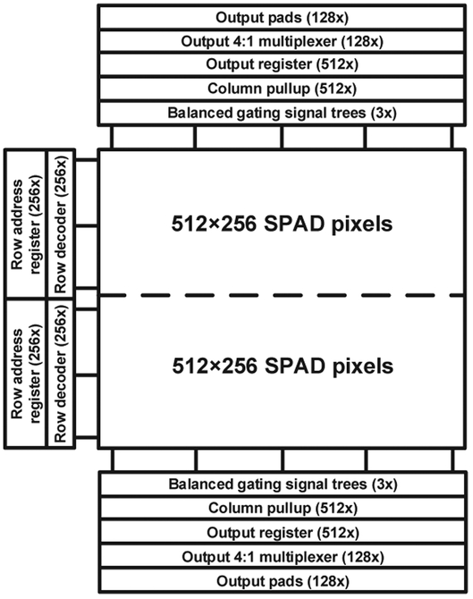
The readout architecture design choices were determined by the sensor’s target specifications. The most important requirement was the ability to read a 1-bit full frame in less than 10.2 μs, which corresponds to a frame rate of 97.7 103 frame-per-seconds (97.7 kfps). This value corresponds to 24 fps when using a 12-bit depth, which is compatible with the real-time data acquisition requirements of FLIM and conventional low-light-level imaging. The second requirement was to use no more than 128 output pads per 512×256 sub-array, due to restrictions related to chip area and the typical number of pins of commercially available FPGA modules. As a result, we decided to employ 4:1 multiplexers for each output pin, enabling to sequentially read 4 columns during the readout of one row. In addition, 1-bit registers implemented by D-flip-flops, store the binary photon count of each column output line during the readout of a row.
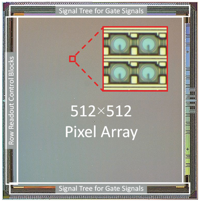
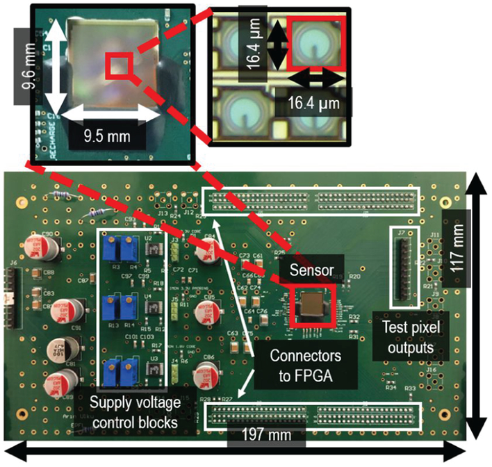
The photomicrograph and the main components of the sensor are displayed in Fig. 5, while the detailed sensor block diagram is shown in Fig. 6. The sensor consists of two identical 512×256 sub-arrays, which are juxtaposed on the chip. The readout of SwissSPAD2 is based on the architecture of its predecessor, SwissSPAD [23]. Readout blocks of each row are located on the left of the array. These blocks decode an 8-bit code that is provided by an external counter. Each value of the code enables the readout of a different row in a single sub-array. When the value of the code increments, the readout of the next row starts, and the memory of the last row is erased using a reset signal generated on the falling edge of the readout. The speed of the counter determines the overall readout speed of the sensor.
The gating signals are distributed from the input pad to the bottom pixel of each column via balanced signal trees, so as to minimize the skew of gating signals within a single row. The gate distribution scheme, which enables the shift of the gates by <40 ps using phase shifters, is synchronous to an external laser trigger, and is independent from the system clock driving the readout blocks.
D. System Architecture
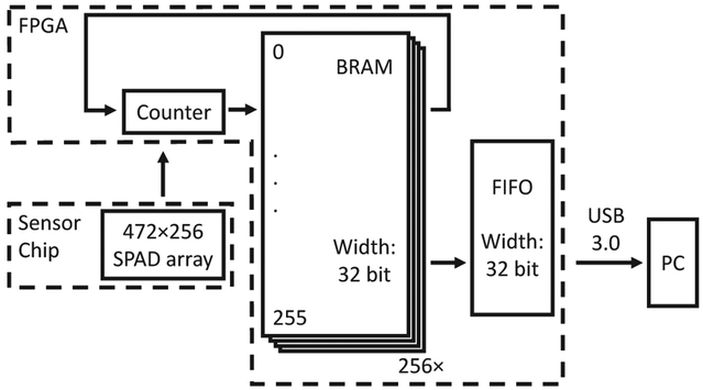
The most important target of the system is to transfer the total photon count of all pixels to the PC while the sensor is operating continuously at its maximum readout speed. The most advanced version of the firmware that was successfully tested so far is shown in Fig. 7. In this configuration, the counts of each pixel are stored in a dedicated address in the BRAM blocks, and dynamically edited after each 1-bit frame readout of the sensor chip. Since photon accumulation is performed in the Kintex 7 FPGA, the size of the data transferred decreases significantly, obviating the USB 3.0 bandwidth limit, which is typically the throughput bottleneck of the system. This architecture currently does not meet the ultimate target of continuous data acquisition due to its two “blind” periods. Firstly, the sensor is insensitive to photons during readout due its global shutter mode operation. Secondly, the data acquisition of the sensor must be paused during the transfer of the 8-bit data inside the PC from the RAM to the storage device (SSD). The firmware was successfully tested up to a 1-bit readout speed of 97.7 kfps. However, during most of the measurements reported in this paper, an older version of this firmware without FPGA-based photon counting feature was used.
III. Performance Characterization
A. Setup
A camera test module with an FPGA development board was designed to characterize SwissSPAD2 and use it for FLIM. This module, shown in Fig. 8, is optimized for testability. Due to a limitation imposed by the number of I/O pins on the FPGA, only 256 rows and 472 columns are tested in this module. To be able to probe each control signal of the chip, a breakout board was introduced between sensor and FPGA, at the expense of slower signal propagation and higher jitter.
B. Static Performance
Dark counts determine the lower bound of dynamic range. In addition, the non-uniform spatial distribution of DCR limits the overall photon counting uniformity in large arrays. As shown in Fig. 2, the p-i-n SPAD employed in this sensor achieves among the lowest noise levels in the literature [14]. An analysis of DCR spatial distribution in SwissSPAD2 (Fig. 9), performed in approximately 25°C without sensor cooling, shows approximately 1% of hot pixels, i.e. pixels in which DCR is over 2 orders of magnitude higher than the median. The scattered distribution of hot pixels in the array, visible in Fig. 9A, shows that masking or blending of hot pixels can be done without affecting image quality. Compared to other large format SPAD sensors, the hot pixel percentage in SwissSPAD2 is significantly lower [30].
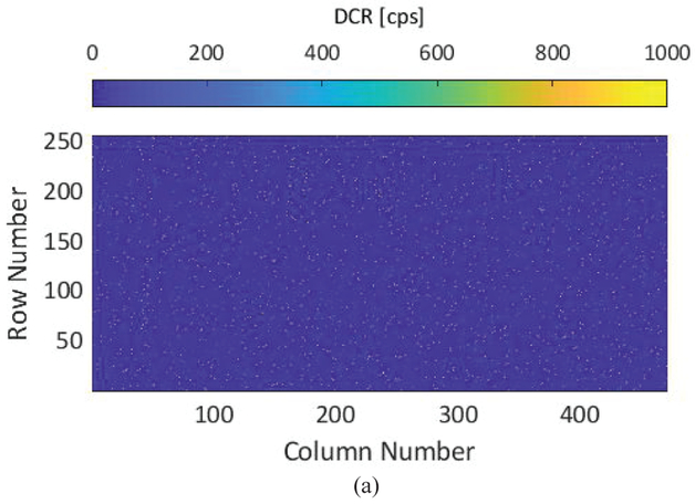
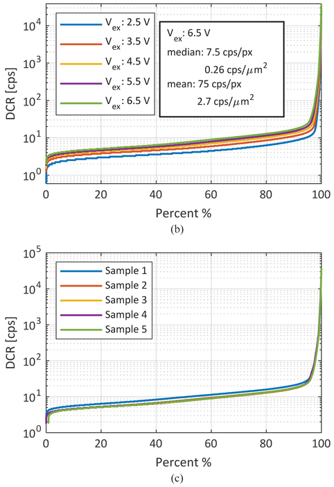
Dark count rate (DCR) performance of the sensor, (a) DCR map showing the distribution of hot pixels across the 472×256 array, (b) Population distribution of the array under 5 different excess bias voltages, (c) Population distribution of the array measured with 5 different camera modules (Vex=6.5V).
C. Dynamic Performance
Photon response uniformity (both spatial and temporal) is a key performance indicator in large format image sensors. The signal-to-noise ratio (SNR) curve for a single pixel, shown in Fig. 10, indicates Poisson-limited temporal performance. The spatial uniformity, quantified by the SNR (average photon count divided by the standard deviation of photon counts over the array) is lower than the Poisson-limited SNR for low illumination levels due to DCR non-uniformity (hot pixels). At higher illumination levels, the relative contribution of DCR non-uniformity decreases and the spatial SNR reaches Poisson-limited performance, indicating very low photon-response non-uniformity. At very high illuminations, saturation of the sensor reduces again the standard deviation of the counts to levels below the Poisson characteristics [31, 32]. This artificial increase of the SNR is due to the unequal distribution of missed photons. A higher count number has a higher probability to be suppressed due to the response saturation. This leads to a decrease in the overall dispersion of the photon count distribution.
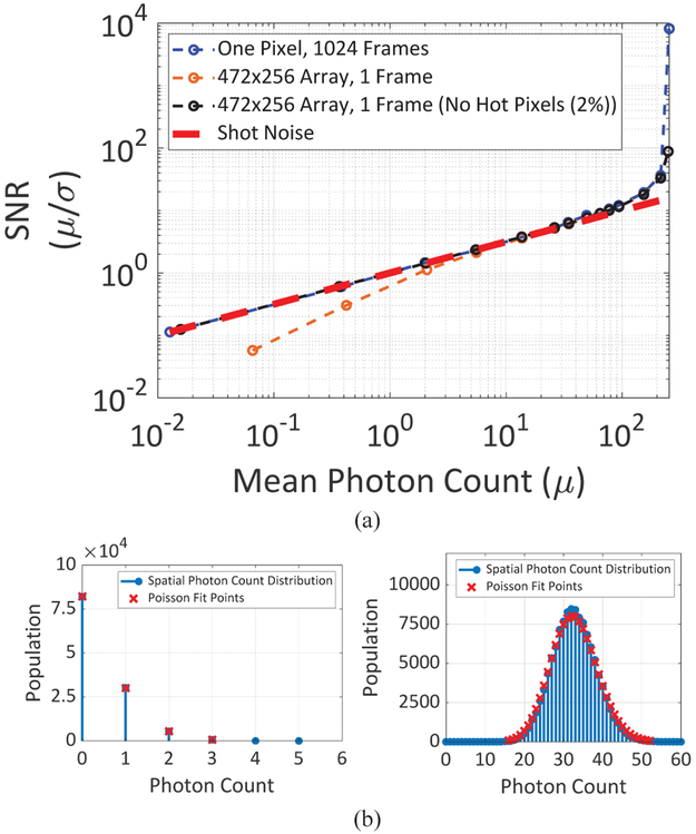
(a) Temporal and spatial SNR of SwissSPAD2 under different illumination levels, (b) Photon count distributions at low and high counts with Poisson fit points. 8-bit images were captured at a frame rate of 0.9 fps.
SwissSPAD2 is designed to operate at high frame rates (in order to capture fast dynamics) and to achieve high dynamic range. Presently, it can reach a maximum 1-bit frame rate of 97.7 kfps. Fig. 11 shows 4-bit and 8-bit images of a rotating fan recorded at 4.4 kfps and 274 fþs, respectively. These images were captured in global shutter mode: the gate opening for exposure and 1-bit frame readout were performed sequentially. Therefore, the frame rate is slower than the maximum reported value of 97.7 kfps, which can be achieved in the rolling shutter mode, where the exposure occurs during the continuous readout. The total exposure for each 1-bit frame was 950 ns, which was achieved by opening a 95 ns-wide gate 10 times with 400 ns periods before the 10.2 μs 1-bit readout.
The power consumption of SwissSPAD2 was measured with the 97.7 kfþs global shutter firmware with 10×95 ns gates per 1-bit image and 6.5 V Vex. The contributions of different parts of the chip under three different illumination settings are shown in Table I. The two settings that are typically preferred are the “dark” and “bright” modes, in which the total power is 26.7 mW and 700 mW, respectively. The “saturation” regime is not a target operation mode; however it was added for a comprehensive analysis of the relative activities of various parts. The average current of a SPAD is proportional to the number of avalanche events, including the events that are not stored in the memory as a result of saturation or gating. On the other hand, the switching frequencies of the I/O blocks depend on the output pattern as well as the average photon count. Therefore, the I/O power consumption is higher when high and low pixels are scattered in the image, and lower when there is high spatial intensity uniformity.
TABLE I
Power Consumption Summary
| Dark (μ<l/255) | Bright (μ=122/255) | Saturation (μ=255/255) | |
|---|---|---|---|
| Sensor Core | 20.1 mW | 36.3 mW | 45.3 mW |
| I/O Blocks | 6.6 mW | 600 mW | 16.5 mW |
| SPADs | ~0 mW | 62 mW | 1,710 mW |
| TOTAL | 26.7 mW | 700 mW | 1,770 mW |
The characteristics of the gate window and its uniformity across the array are key metrics in time-resolved imaging, ultimately limiting the accuracy and precision of fluorophore lifetimes. The gate characteristics of SwissSPAD2 under two different settings are presented in Fig. 12 and Fig. 13. In Fig. 12, the gate characteristics of the 5.75 ns gate on the 472×256 pixel array are presented. This experiment was performed using a 790 nm pulsed laser with 20 MHz pulse repetition frequency (PRF). The laser pulse was synchronized to a 20 MHz trigger signal which was generated by the FPGA of the camera system. The time-scanning was achieved by shifting the phase of the gate and recharge signals with respect to the laser trigger from the FPGA. The shortest achievable gate window was 5.75 ns, with a 250 ps rising and an 344 ps falling edge skew. In Fig. 13, the characterization of the gate with the lowest skew on the 472×256 array is presented. The PRF was kept at 20 MHz and the gate length was set to approximately half of the laser period to decrease the gate skew; by choosing the lowest possible switching frequency of the signal tree inverters, the average voltage drop during the switching was minimized. To achieve lower jitter, an internal trigger from the laser controller was used to generate the gate signals.
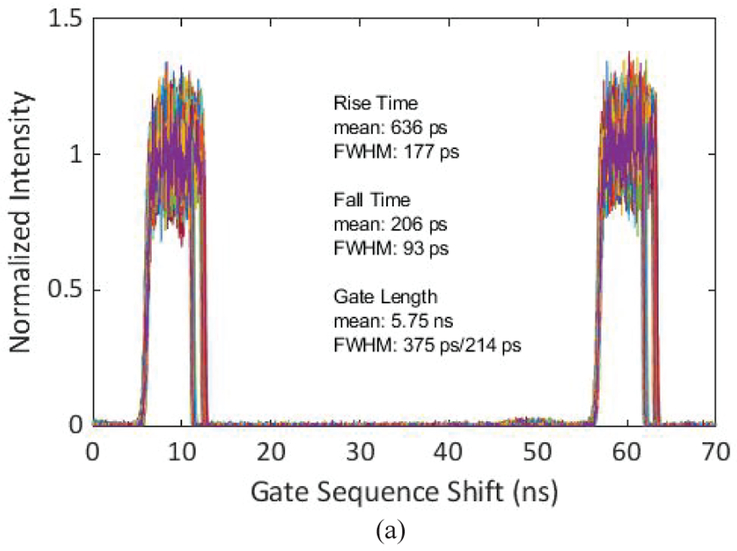
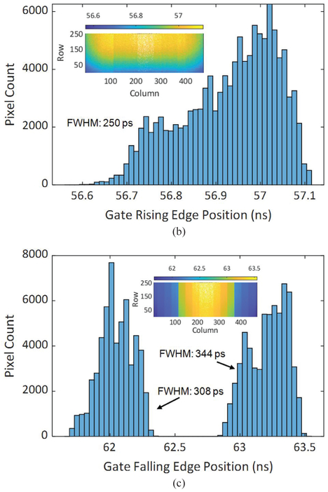
Gating characterization of the shortest achieved gate with 5.75 ns length, (a) Gate window shape of each pixel in the array, (b) distribution of gate window rising edge position, and (c) distribution of gate window falling edge position. 3% of the pixels were removed from the analysis due to a non-existent gate window.
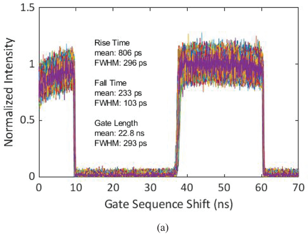
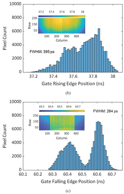
Gating characterization of the gate with the lowest achieved skew with 22.8 ns length, (a) Gate window shape of each pixel in the array, (b) distribution of gate window rising edge position, and (c) distribution of gate window falling edge position.
The gating characterization data show that the rising edge of the gate is slower than the falling edge. This mismatch is due to different hardware behavior affecting the rise and fall times. The gate fall time is determined by the switching speed of the gate transistor (T5) in the pixel, whereas the rise time is determined by the speed of discharging the SPAD capacitor after the recharge transistor (T3) switches on, which is significantly slower than the switching time of a transistor. The existence of a minimum gate length is mainly due to the rise and fall time durations of the “recharge” and “gate” signals of the sensor chip that set the boundaries of the gate window. As these signals propagate across the array, their toggling speed decreases due to the parasitic resistance and capacitance of the long, narrow wires. In Fig. 12 (c) and Fig. 13 (c), the two peaks in the gate falling edge position distribution are caused by the horizontal gate skew, which is a result of voltage drop in the gate signal trees. This skew is most apparent between the columns 127–128, and 383–384, as a result of the signal tree architecture. The vertical skew which is the dominant source of skew in the rising edge is caused by the propagation of the signals from the bottom of the array to the top using long wires. The skew can be offset by performing instrument response function (IRF) characterization before the time-resolved imaging tests, as demonstrated in the following sections.
IV. Fluorescence Intensity Imaging Microscopy
Thanks to its large array format, low DCR, and high PDP in a wide spectrum, SwissSPAD2 is suitable for widefield fluorescence microscopy. In this section, we present the results of two fluorescence intensity microscopy experiments with SwissSPAD2. The first experiment compares the signal-to-noise ratio (SNR) of fluorescence intensity images of beads captured by SwissSPAD2 and by a sCMOS camera. A 2D array of beads labeled with 5, 25 and 50 μg/mL Alexa 647 solution was captured with both cameras sequentially with equal exposure times of 25 ms. Intensity profiles that include all three concentrations are extracted as grayscale images. The SNR was calculated from the ratio between the mean value of a peak in the profile and the standard deviation of the noise floor. SwissSPAD2 was operated at 5.5 V excess bias and in the rolling shutter mode; 100 ns gates were repeated in every 400 ns. The exposure time was adjusted by choosing the frequency of the readout; 25 ms gate was achieved by activating every 4 readout cycle.
Fig. 14 shows the normalized intensity profiles obtained with both cameras, and the ratio between their SNR. The intensity profile of SwissSPAD2 was generated after the removal of hot pixels and DCR correction. A SNR ratio of 4 (and sensitivity ratio of 16) was found by this analysis. The ratio obtained by the experiments is comparable to the ratio between the quantum efficiency (QE of 77%) of the sCMOS and the PDE (PDP of 35% and fill factor of 10.5%) of SwissSPAD2. The slightly lower ratio is explained by the elimination of readout noise and analog non-uniformity with SwissSPAD2. The sensitivity ratio was derived from the SNR ratio instead of being directly calculated due to the complexity of a reliable conversion between the electron count of an sCMOS and a photon count of a SPAD.
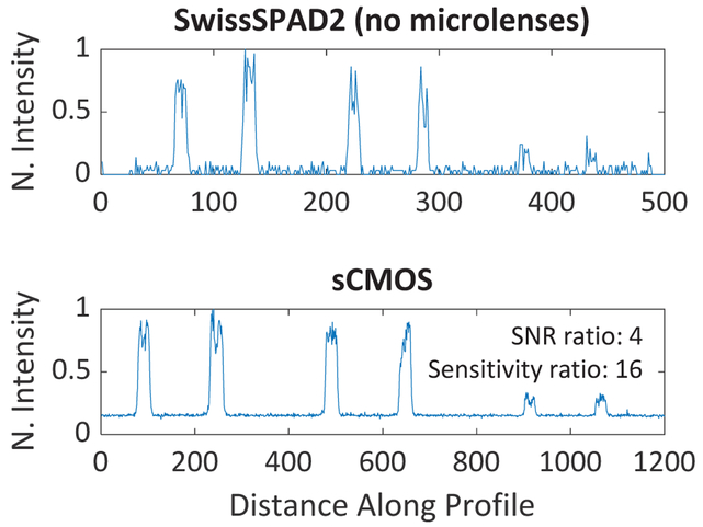
Intensity profiles of beads with 3 different fluorophore concentrations captured with Hamamatsu ORCA-Flash4.0 V2 sCMOS camera and SwissSPAD2 without microlenses. 625 nm LEDs were used for the excitation of the samples.
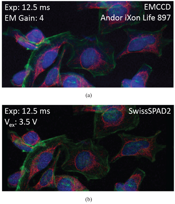
We also performed multicolor imaging with SwissSPAD2 to compare its performance with an EMCCD camera, which is typically used for this application. In this experiment, HeLa cells labeled with DAPI, Alexa 488, and Alexa 555 were successively excited with three different wavelengths (Xenon lamp source filtered by bandpass filters centered at 387 nm, 485 nm and 560 nm) and captured with appropriate emission filters by an EMCCD camera and SwissSPAD2, sequentially, with equal exposure times. To achieve high photon efficiency during long exposures with SwissSPAD2, the gate was opened for ~200 ns during the readout of each row in rolling shutter mode. As a result, 255 1-bit images were captured with a total gate exposure of 12.5 ms (49 μs exposure per 1-bit frame). SwissSPAD2 images were first corrected for pile-up, followed by hot pixels (381 for blue, and 347 pixels for green and red) interpolation and DCR subtraction. The RGB images in Fig. 15 were constructed from the intensity images of three different emission channels normalized to full contrast, i.e. the highest intensity in each channel is set to the maximum RGB channel value of 255. This adjustment was performed to eliminate the visual effects of photobleaching and sensitivity difference to different wavelengths.
V. Fluorescence Lifetime Imaging Microscopy
In this section, we report the performance of SwissSPAD2 for widefield FLIM. The data acquisition method in time-gated FLIM is illustrated in Fig. 16. A fixed-size gate is swept across the laser period by shifting its delay with respect to the laser pulse [29, 33]. The photon count of each gate position is obtained by capturing a series of 1-bit frames for each position and accumulating their intensity values outside the chip. The number of 1-bit frames per gate position is user-selectable based on the dynamic range and data acquisition speed requirements. Finally, the gate response is converted into fluorescence lifetime by various methods. The minimum resolvable lifetime and the accuracy of the extracted result are determined by the time delay between two subsequent gate positions, the gate edge jitter, i.e. the temporal uncertainty of the gate edge position of a single pixel which cannot be corrected due to its stochastic nature and to a larger extent, the SNR. The minimum gate shift supported by the current SwissSPAD2 system is 18ps, which is limited by the fine phase shifting capability of the FPGA clock generator IP block executing this task. Depending on the target lifetime and the required accuracy, larger gate steps can be chosen to minimize the total data acquisition time, which also reduces the computational intensity of data processing.
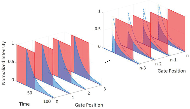
Conceptual illustration of time gating in SwissSPAD2. The delay between subsequent gate positions is a small fraction of the gate length. Each gate window is sensitive to a different part of the fluorescence decay. The characteristics of the decay are derived from the total photon count detected by each gate position. The reduced fluorescence intensity over time is caused by the bleaching effect in some samples after long exposures to the excitation light. In the samples used in this FLIM experiment, no significant bleaching was observed.
The samples used in this FLIM experiment consist of three fluorescent solutions: two water-soluble organic dyes (Cy3B and Rhodamine 6G, Sigma Aldrich), and a water-soluble semiconductor quantum dot sample (Qdot 655 Streptavidin, ThermoFisher Scientific). A 532 nm, 100 picosecond wide pulsed laser with 20 MHz pulse repetition rate (LDH-P-FA-530XL, PicoQuant, Germany) sent in epi-illumination into the 60X NA 1.45 oil immersion objective lens of an inverted microscope (IX71, Olympus) through a 532 nm dichroic mirror, was used for widefield excitation of a ~10 μL drop sealed between to glass coverslips. The emission signal was filtered using appropriate bandpass filters (dyes: centered at 582, bandwidth: 75 nm, Qdot: long pass 610 nm). 125 gate positions with 22.8 ns gate length and a 428.6 ps offset between consecutive gates were used, each gate sequence being repeated 1,024 times to obtain sufficient dynamic range. The response of the acquisition chain, or instrument response function (IRF), was obtained by collecting the laser signal reflected off a clean glass coverslip, with the emission filter removed.
Fig. 17 shows a representative decay from each sample, corresponding to a square region of interest (50×50 pixels) in the center of the array. Decays were fitted to a single-exponential integrated with a gate profile provided by the measured periodic IRF, using a standard Levenberg-Marquard algorithm implemented in a custom LabVIEW software (AlliGator [34]). Single-exponential fits of the R6G solution and QD655 decays are shown in Fig. 17(a) and (b), respectively.
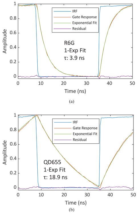
Fluorescence lifetime extraction of (a) Rhodamine 6G (R6G) solution, and (b) quantum dots (QD655) by fitting the decay by a single exponential integrated over a gate profile provided by the IRF sample, and pile-up correction [34]. The signal shown corresponds to the total signal within a square region of 50×50 pixels.
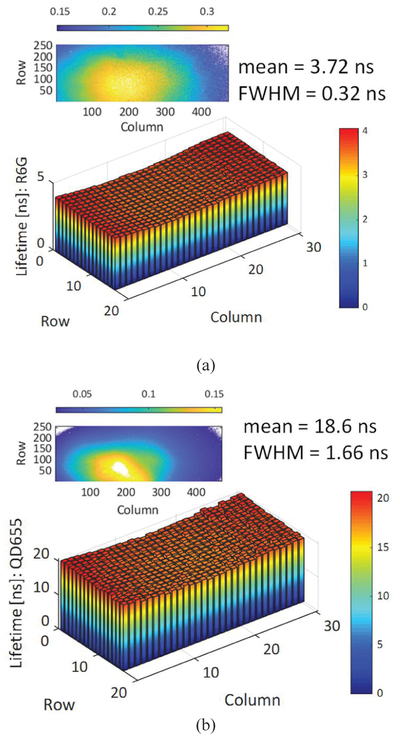
Decay fitting analysis is computationally demanding and therefore was limited to individual regions of interest (ROI) only. To compute a lifetime map of each sample, we resorted to phasor analysis. Phasor analysis, thanks to its linear algebraic lifetime calculation method, drastically reduces the computational complexity of single and multi-exponential lifetime analysis, and is therefore suitable for real-time widefield FLIM applications [35, 36, 37]. In this approach, each decay is replaced by the coefficients of a single term of its Fourier series and represented in a so-called phasor plot (Fig. 18) [38]. Single-exponential decays are located on a semicircle (the so-called universal circle or UC) with a simple correspondence between each decay’s phasor location and its lifetime. Fig. 18 shows that using the average phasor of the Cy3B solution for calibration, and attributing to it the 2.5 ns lifetime obtained by fitting, the phasor of the other dye (Rhodamine 6G) is located on the UC as well (fitted lifetime of 3.9 ns), while the Qdot sample is located close to it (fitted lifetime: 18.9 ns). This is consistent with the multi-exponential decays characteristic of semiconductor nanocrystals. The FLIM image constructed with phasor analysis is shown in Fig. 19, as well as the intensity image of the same sample for comparison. Pile-up was corrected using a correction formula [20]. Faster readout speed in future designs will further minimize the pile-up effect.
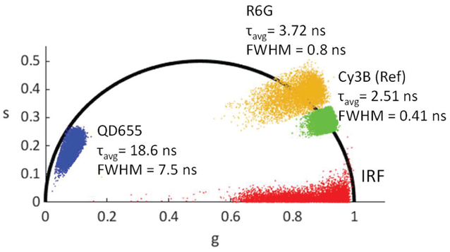
Phasor plot (20 MHz harmonic) of quantum dots (QD655), Rhodamine 6G (R6G) solution, Cy3B solution for reference, and the IRF. After calibration, the phasor points are transferred to the region around the semicircle, from which the phase lifetime is extracted.
VI. State-of-the-Art Comparison
The performance of SwissSPAD2 was compared to other large-format SPAD imagers in the literature in Table II. SwissSPAD2 has the largest array format and the lowest median DCR compared to other SPAD imagers. The relatively lower native fill factor was in part due to the lack of well sharing chosen to achieve SPAD pitch uniformity throughout the array. The main limitation of the timing performance is introduced by the gate rise/fall times, which determine the jitter of the gate window. Performance degradation due to relatively slower gate rise time can be prevented by scanning the entire decay with a long gate using only the falling edge. This method can be applied only if the gate width is at least several times longer than the target lifetime. This method allows the overall timing resolution of the system to be determined by the mean fall time of the gate, which is comparable with the timing resolution of the SPAD and the jitter of the gate signal. The gate skew on the falling edge is dominated by the boundaries between columns 127–128 and 383–384, which manifest itself as two distinct peaks in Fig. 13 (c). These differences can be corrected for during decay fitting or phasor analysis by using the proper IRF for gate integration or calibration in order to mitigate the effects of the skew. The voltage drop in the signal trees, which is caused by the chip layout constraints, increases the gate rise/fall times and the minimum achievable gate length. This factor can be eliminated by changes in the layout in the future version of the chip.
TABLE II
State-of-the-Art Comparison of Large-Format SPAD Image Sensors
| This Work | [21] [39] | [12] | [40] | [41] | [30] | [23] | |
|---|---|---|---|---|---|---|---|
| Process Technology | 180 nm CMOS | 130 nm CIS | 350 nm HV CMOS | 350 nm HV CMOS | 130 nm CIS | 130 nm CIS | 350 nm |
| Array Format | 512×512 | 320×240 | 160×120 | 32×32 | 256×256 | 256×256 | 512×128 |
| Pixel Pitch | 16.38 μm | 8 μm | 15 μm | 25 μm | 8 μm | 16 μm | 24 μm |
| Fill Factor (Nominal) | 10.5% | 26.8% | 21% | 20.8% | 19.6% | 61% | 5% |
| Fill Factor (With Microlenses) | - (>50% expected) | 50% | - | - | - | - | 60% |
| Chip Size | 9.5×9.6 mm2 | 3.4×3.1 mm2 | 3.42×3.55 mm2 | - | 3.5×3.1 mm2 | 5×5 mm2 | 13.5×3.5 mm2 |
| Max. PDP | ~50% @520 nm (Vex = 6.5 V) | 39.5% @480 nm (Vex = 1.5 V) | - | - | - | 39.5% @480 nm (Vex = 3 V) | 46% @490 nm (Vex = 4 V) |
| Median DCR | 7.5 cps/px 0.26 cps/μm2 (Vex = 6.5 V) | 47 cps/px 2.7 cps/μm2 (Vex = 1.5 V) | 580 cps/px 12.3 cps/μm2 (Vex = 2.5 V) | 500 cps/px 3.8 cps/μm2 (Vex = 5 V) | 50 cps/px 4.0 cps/μm2 (Vex = 2 V) | 6.2 kcps/px 40 cps/μm2 (Vex = 1.5 V) | 366 cps/px 12.7 cps/μm2 (Vex = 4.5 V) |
| Readout Noise | 0 | 0.168e− | - | - | - | Negligible | 0 |
| Uniform SPAD Pitch | Yes | No | No | - | - | No | Yes |
| Maximum Frame Rate | 97.7 kfps (1 bit) | 16 kfps (1 bit) | 486 fps (5.4 bit) | 50 fps (1.5 V analog output) | 4 kfps (3-bin histogram) | 100 kfps (1 bit) | 156 kfps (1 bit) |
VII. Conclusions
This paper describes the design and characterization of a 512×512 pixels time-gated binary SPAD image sensor – the largest format reported to date – in standard CMOS technology. SwissSPAD2 features state-of-the-art DCR and PDP with a wide spectral response, high speed read-out (up to 97.7 kfps), as well as the possibility of gating each pixel with windows as short as 5.75 ns thanks to a fully integrated gating option. This solution is actually the key enabler of time-resolved imaging on a sensor of this size. Thanks to its large field of view and high SNR, SwissSPAD2 is thus suitable for widefield fluorescence microscopy, as demonstrated with preliminary results on biologically relevant samples stained with multiple dyes. In addition, we have also shown that our single-photon counting image sensor with long and slightly overlapping time gates provides an all solid-state platform to perform widefield fluorescence lifetime analysis. Measurements on organic dyes and semiconductor quantum dots were carried out as a proof of principle, thereby providing an experimental validation of the proposed gating scheme. Future versions of the sensor will feature the addition of microlenses to increase the overall sensitivity and optimized high-speed firmware, making the proposed sensor a potential low-cost alternative to commercially available scientific time-resolved imagers.
Acknowledgment
The authors would like to thank Dr. Nicolas Descharmes (EPFL, OPT Lab), Dr. Arne Seitz (EFPL, BIOP), Andrei Ardelean (EPFL, AQUA Lab), and Dr. Joonhyuck Park (UCLA, Dept, of Chemistry and Biochemistry) for their valuable contributions.
This work was supported in part by Swiss National Science Foundation, Netherlands Organization for Scientific Research project 13916, HFSP grant RGP0061/2015 and NIH grant GM 095904 and CRCC grant CRR-18–523872 (UCLA). RA is supported by a Excelling Post-Doctoral Students scholarship from the Council of Higher Education, Israel.
Biographies
Arin C. Ulku received the master’s degree from the Delft University of Technology, Delft, Netherlands, in 2016. He is currently working towards his Ph.D. in the AQUA Laboratory, École Polytechnique Fédérale de Lausanne, Neuchâtel, Switzerland. His main research interests are single-photon counting time-correlated image sensors for fluorescence microscopy applications.

Claudio Bruschini (MΊ2 SMΊ7) received the Laurea degree in physics from the University of Genoa, Genoa, Italy, in 1992, and the Ph.D. degree in applied sciences from Vrije Universiteit Brussel, Brussels, Belgium, in 2002. He is currently a Scientist with EPFL’s Advanced Quantum Architecture Laboratory. His scientific interests have spanned from high energy physics and parallel computing in the early days, to challenging sensor applications in humanitarian demining, concentrating since 2003 on quantum photonic devices, high-speed and time-resolved 2D/3D optical sensing, as well as applications thereof (biophotonics, nuclear medicine, basic sciences, security, ranging).

Ivan Michel Antolović received his M.S. degree (cum laude) from University of Zagreb in 2012, and his PhD degree from TU Delft in 2018. He has been with EPFL, Neuchâtel, since 2018. His work focuses on large format photon counting SPAD imagers and small format time correlated SPAD imagers for microscopy applications.
Yung Kuo received MS degree in chemistry from National Taiwan University in 2012. She is currently a PhD candidate in the Dept, of Chemistry and Biochemistry at the University of California, Los Angeles. Her doctoral research focuses on developing and characterizing semiconductor nanorods for voltage sensing.
Rinat Ankri received her PhD degree from Bar Ilan University, Israel, in 2013. She is currently a postdoctoral fellow at the University of California, Los Angeles, in Prof. Shimon Weiss lab. Her main research interests include bio molecular and fluorescence lifetime imaging through turbid medium.
Shimon Weiss received the B.Sc. degree in 1984 and the D.Sc. degree in 1989 from the Technion, Israel Institiute of Technology in Electrical Engineering. His postdoctoral training was at AT&T Bell Laboratories. He was a Staff Scientist at Lawrence Berkeley National Laboratory between 1991 and 2001. In 2001, he joined UCLA as a Full Professor. He holds the Dean M. Willard Chair in the Department of Chemistry & Biochemistry and the Department of Physiology. He is a Fellow of the Optical Society of America, received the 2001 Michael and Kate Barany Biophysical Society Award, the 2006 Rank Prize in opto-electronics, and the Humboldt Research Award in 2012. His lab has been working on ultrasensitive single molecule spectroscopy methods and applications, conformational dynamics of biomolecules, superresolution imaging, and introduction and optimization of quantum dots to biological imaging.
Xavier Michalet received the doctorate degree in science from University Paris VII, Paris, France, in 1994. His research interests include developing new techniques to improve the sensitivity, throughput and accuracy of single-molecule fluorescence studies.

Edoardo Charbon (SM’10 F’17) received the Diploma degree from ETH Zurich, Zurich, Switzerland, in 1988, the M.S. degree from the University of California at San Diego, La Jolla, CA, USA, in 1991, and the Ph.D. degree from the University of California at Berkeley, Berkeley, CA, USA, in 1995, all in electrical engineering and computer sciences. He has been with the École Polytechnique Fédérale de Lausanne (EPFL), Lausanne, Switzerland, since 2002. From 2008 and 2016 he was Chair of VLSI design at TU Delft, Delft, Netherlands. His research interests include single-photon and photon-counting imaging, cryogenic electronics, and quantum computing. Dr. Charbon is a member of the Kavli Nanoscience Institute Delft, a distinguished lecturer of the IEEE Photonics Society, and a fellow of the IEEE.
References
Full text links
Read article at publisher's site: https://doi.org/10.1109/jstqe.2018.2867439
Read article for free, from open access legal sources, via Unpaywall:
https://ieeexplore.ieee.org/ielx7/2944/8383723/08449092.pdf
Citations & impact
Impact metrics
Article citations
Scintillation event imaging with a single photon avalanche diode camera.
Commun Eng, 3(1):135, 18 Sep 2024
Cited by: 0 articles | PMID: 39294245 | PMCID: PMC11411079
High-throughput fluorescence lifetime imaging flow cytometry.
Nat Commun, 15(1):7376, 04 Sep 2024
Cited by: 0 articles | PMID: 39231964 | PMCID: PMC11375057
Underwater Single-Photon 3D Reconstruction Algorithm Based on K-Nearest Neighbor.
Sensors (Basel), 24(13):4401, 07 Jul 2024
Cited by: 0 articles | PMID: 39001180 | PMCID: PMC11244583
A 64 × 128 3D-Stacked SPAD Image Sensor for Low-Light Imaging.
Sensors (Basel), 24(13):4358, 05 Jul 2024
Cited by: 1 article | PMID: 39001137 | PMCID: PMC11244227
Multiplexed near infrared fluorescence lifetime imaging in turbid media.
J Biomed Opt, 29(2):026004, 29 Feb 2024
Cited by: 0 articles | PMID: 38425720 | PMCID: PMC10902792
Go to all (40) article citations
Similar Articles
To arrive at the top five similar articles we use a word-weighted algorithm to compare words from the Title and Abstract of each citation.
Phasor-based widefield FLIM using a gated 512×512 single-photon SPAD imager.
Proc SPIE Int Soc Opt Eng, 10882:108820M, 22 Feb 2019
Cited by: 3 articles | PMID: 33859449 | PMCID: PMC8046026
A 65k pixel, 150k frames-per-second camera with global gating and micro-lenses suitable for fluorescence lifetime imaging.
Proc SPIE Int Soc Opt Eng, 9141:914109, 01 Apr 2014
Cited by: 2 articles | PMID: 28626292 | PMCID: PMC5471623
Photon-Counting Arrays for Time-Resolved Imaging.
Sensors (Basel), 16(7):E1005, 29 Jun 2016
Cited by: 8 articles | PMID: 27367697 | PMCID: PMC4970055
Single Photon Avalanche Diode Arrays for Time-Resolved Raman Spectroscopy.
Sensors (Basel), 21(13):4287, 23 Jun 2021
Cited by: 3 articles | PMID: 34201576 | PMCID: PMC8272195
Review Free full text in Europe PMC
Funding
Funders who supported this work.
Dutch Research Council (NWO) (1)
Grant ID: 13916
Excelling Post-Doctoral Students Scholarship from the Council of Higher Education, Israel
HFSP (1)
Grant ID: RGP0061/2015
NIGMS NIH HHS (1)
Grant ID: R01 GM095904
NIH (2)
Grant ID: GM 095904
Grant ID: CRR-18-523872
Netherlands Organization for Scientific Research Project (1)
Grant ID: 13916
Swiss National Science Foundation (1)
Grant ID: 166289
