Abstract
Free full text

Ultra-smooth glassy graphene thin films for flexible transparent circuits
Associated Data
Abstract
Large-area graphene thin films are prized in flexible and transparent devices. We report on a type of glassy graphene that is in an intermediate state between glassy carbon and graphene and that has high crystallinity but curly lattice planes. A polymer-assisted approach is introduced to grow an ultra-smooth (roughness, <0.7 nm) glassy graphene thin film at the inch scale. Owing to the advantages inherited by the glassy graphene thin film from graphene and glassy carbon, the glassy graphene thin film exhibits conductivity, transparency, and flexibility comparable to those of graphene, as well as glassy carbon–like mechanical and chemical stability. Moreover, glassy graphene–based circuits are fabricated using a laser direct writing approach. The circuits are transferred to flexible substrates and are shown to perform reliably. The glassy graphene thin film should stimulate the application of flexible transparent conductive materials in integrated circuits.
INTRODUCTION
In recent years, great attention has been paid to the exploitation of flexible transparent conducting materials for applications in wearable electronics, flexible displays, touch panels, and solar cells (1–5). Typically, metal (Ag and Cu) nanowire networks/grids show great promise in terms of flexibility, transparency, and conductivity (4, 6–9). The development of Cu nanowire networks reduces costs as compared to that of noble metal networks. Moreover, efforts to develop core/shell structures greatly improve stability issues (8). In addition, graphene, which is a two-dimensional monolayer of carbon atoms in a honeycomb lattice, is one of the most flexible and transparent conducting materials (10, 11). Large-area and high-quality graphene thin films are successfully synthesized using chemical vapor deposition (CVD) over metal substrates (Cu and Ni) (12, 13); in particular, 1.5-inch single-crystal graphene can be deposited through a localized feeding approach over a Cu-Ni alloy substrate (14). Efforts to improve transfer strategies (15, 16) or to deposit graphene directly on insulating substrates (SiO2, SrTiO3, MgO, and Al2O3) (15, 17–20) have been made to overcome transfer-induced issues, such as cracks and wrinkles. Improvement in the large-scale homogeneity and smoothness of graphene will advance the use of its thin film in wafer level integrated electronics and meet high-standard requirements in terms of uniformity, connectivity, and roughness (<1 nm) in the electronic industry.
Here, a type of ultra-smooth glassy graphene thin film was deposited on a SiO2 (quartz) substrate using an aqueous solution approach. It is found that glassy graphene is in an intermediate state between glassy carbon and graphene and inherits both of their excellent properties. From a structural perspective, glassy graphene is better crystallized than glassy carbon but still has a distorted lattice plane as compared with graphene. As for the properties, glassy graphene exhibits good chemical and thermal inertness, much like glassy carbon, with conductivity and flexibility comparable to those of graphene. Benefiting from the aqueous solution’s large-scale synthesis system, which we term polymer-assisted deposition (PAD) (21–24), glassy graphene is derived from a molecular precursor coating, resulting in a homogeneous ultra-smooth surface (<0.7 nm) film. Using the heat-curing property of the precursor polymer, the glassy graphene–based circuits are fabricated afterward through infrared laser direct writing. The glassy graphene thin film has great potential applications in flexible transparent integrated electronics.
RESULTS
Structure evolution from glassy carbon to glassy graphene and graphene
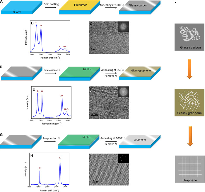
The PAD method is applied to deposit three types of carbon-based thin films under different catalysis conditions. First, a glassy carbon thin film is grown using a spin-coating and annealing process (Fig. 1A). The Raman spectrum of the glassy carbon film (Fig. 1B) shows four characteristic bands, including the D band (1350 cm−1), the G band (1597 cm−1), the 2D band (2695 cm−1), and the D + G band (2935 cm−1). The G and 2D bands indicate the presence of sp2 carbon in glassy carbon, whereas the relatively high D band points to the presence of defects. The microstructure of the glassy carbon thin film is further examined by transmission electron microscopy (TEM). From the high-resolution TEM (HRTEM) data, connected carbon atom rings could be clearly identified but were poorly ordered over larger planar distances (Fig. 1C) (25–27). The diffraction rings from the selected-area electron diffraction (SAED) pattern also confirm that the glassy carbon thin film is partially crystallized and disordered (Fig. 1C, inset). To enhance the crystallization, a layer of Ni thin film is evaporated on the glassy carbon thin film and re-treated via annealing. Because of the catalytic effect of Ni, an intermediate state between glassy carbon and graphene is obtained at 850°C, which we name here as glassy graphene (Fig. 1D). Compared with glassy carbon, the Raman spectrum of glassy graphene shows four similar positioned bands but much sharper peaks (Fig. 1E). One obvious difference is that the I2D/IG ratio of glassy graphene is much higher than that of glassy carbon, increasing from 0.2 to 0.8. Even so, the relative high D band still indicates disorder in glassy graphene. TEM studies show the twisted lattice planes in glassy graphene (Fig. 1F), and the SAED pattern accordingly exhibits a group of bright concentric rings. The Raman, TEM, and SAED analyses conclude that the bent and curved lattice plane is one of the most distinguishing features of glassy graphene (fig. S1), and the glassy state is the intermediate stage of graphene formation. To further graphitize the sample, as expected, graphene evolves from glassy graphene after the annealing temperature is increased to 1000°C. The typical Raman spectrum (Fig. 1H) shows strong 2D and G peaks without a D peak. As is well known, a strong G peak and a disappearing D peak suggest that the sample has a well-ordered graphitic lattice with high crystallinity. Simultaneously, the enhanced I2D/IG ratio points to the sample with a few layers or a single layer of graphene. From the HRTEM lattice image and six reflex spots in the SAED, one can recognize high-quality graphene (Fig. 1I). From the above analysis, the structure evolution of the three types of material can be described (Fig. 1J): Glassy carbon is partially crystallized and disordered, and glassy graphene shows high crystal quality but twisted, bent lattice planes, whereas graphene has perfect lattices.

(A to C) Synthesis process of a glassy carbon thin film and the corresponding Raman spectrum and HRTEM image. The inset to (C) shows the corresponding SAED pattern. (D to F) Synthesis of a glassy graphene thin film and the corresponding Raman spectrum and HRTEM image. The inset to (F) shows the corresponding SAED pattern. (G to I) Synthesis of a graphene thin film and the corresponding Raman spectrum and HRTEM image. The inset to (I) shows the corresponding SAED pattern. (J) Structure evolution from glassy carbon to glassy graphene and graphene.
Ultra-smooth surface of glassy graphene thin films
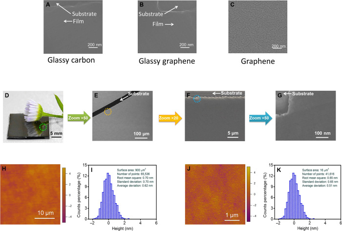
The different and distinct nature of glassy graphene thin films can be attributed to and is inherited from both glassy carbon and graphene. In glassy carbon, carbon atoms link to each other in an isotropy and glassy state without long-range orders, free from crystal domains and grain boundaries. Scanning electron microscopy (SEM) studies (Fig. 2, A and B) show that the PAD-deposited glassy carbon and glassy graphene thin films are dense, smooth, and homogeneous in-plane, implying that glassy graphene retains the morphology of glassy carbon. In contrast, the as-deposited graphene thin film shows obvious cracks (Fig. 2C) and domain boundaries, which might be caused by the reconstruction of the glassy carbon to graphene through a catalytic procedure. Intermediate glassy graphene has both high crystal quality and glassy carbon morphology. In addition, the glassy graphene thin film appears as a shiny and mirror-like surface to the naked eye (Fig. 2D) and is found to be compact, connective, and free from cracks and pores (at the millimeter to nanometer scale), as determined through optical microscopy and SEM (Fig. 2, E to G). Atomic force microscopy (AFM) was applied to further probe the surface morphology of the glassy graphene thin film (Fig. 2, H and J). As anticipated, the AFM studies show that the glassy graphene thin film is compact and connective, as found in our SEM studies. According to the calculated height signal distributions (Fig. 2, I and K), the glassy graphene film has low roughness (<0.7 nm). This notably small roughness of the glassy graphene film is comparable to that found in commercially polished silicon wafers (roughness, <1 nm) and makes the glassy graphene thin film competitive with metal (Ag and Cu) nanowire networks/grids or polycrystalline graphene thin films in terms of surface smoothness.

(A to C) SEM images of glassy carbon (A), glassy graphene (B), and graphene (C). (D) Optical image of a glassy graphene film on a quartz substrate with a daisy on top, showing the reflective surface of the glassy graphene film. (E) Microscopy image of the glassy graphene thin film; the scratch was made to provide contrast between the film and the substrate. (F and G) SEM image of the glassy graphene thin film. The colored dotted circles mark the zoom area respective to the zooming factors in the colored arrows. (H) AFM image (30 μm × 30 μm) of the glassy graphene film. (I) The distribution of heights of the AFM image (H). (J) AFM image (1 μm × 1 μm) of the glassy graphene film. (K) The distribution of heights of the AFM image (J).
Performance of glassy graphene thin film
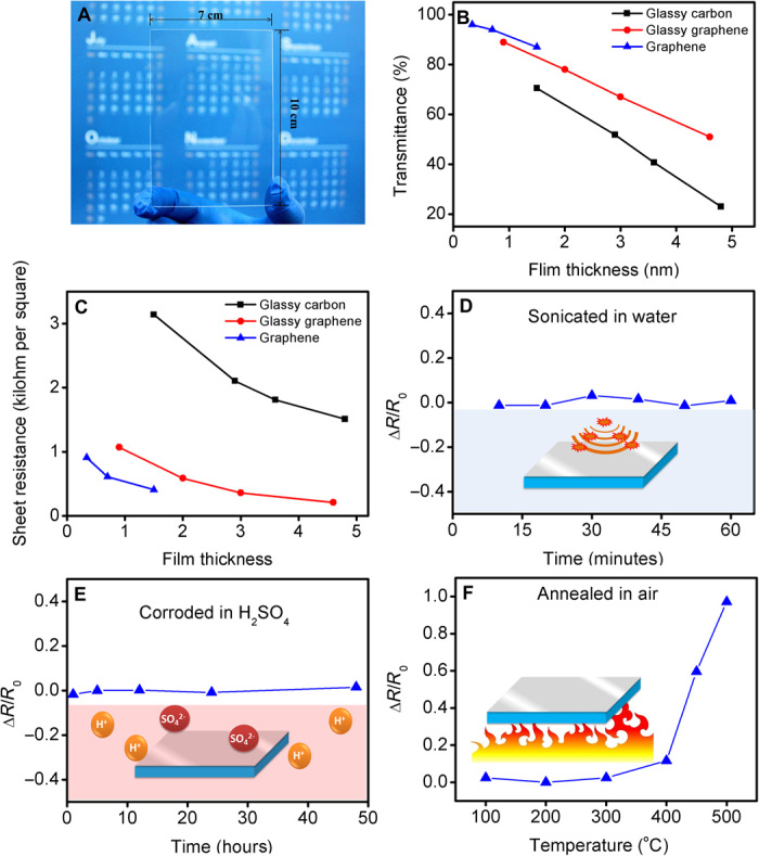
In addition to the structural and morphology properties, the glassy graphene thin film shows conductivity and transparency comparable to those of graphene, whereas the glassy carbon–like mechanical, chemical, and thermal stabilities are retained. The PAD fabrication route offers a large-scale and thickness-tunable production route for the glassy graphene thin film. Figure 3A illustrates a 0.9-nm-thick glassy graphene thin film deposit on a quartz substrate (10 cm × 7 cm). The transparency and sheet resistance of the three types of thin films are studied with respect to their dependence on thickness, as shown in Fig. 3 (B and C). The data show that the performance of glassy graphene is comparable to that of graphene and surpasses that of glassy carbon. The 0.9-nm-thick glassy graphene film has a sheet resistance of 1.075 kilohm per square and a conductivity of 10,335 S/cm. The electrical conductivity of glassy graphene is comparable to that of CVD-grown graphene deposited on insulating substrates (10,000 to 25,000 S/cm) (17–20). In terms of transparency, monolayer graphene shows a transmittance of ~97%, whereas the 0.9-nm-thick glassy graphene and the 1.5-nm-thick glassy carbon show transmittances of ~89 and ~70%, respectively. To test the mechanical reliability of our as-grown glassy graphene thin film, we sonicated the film on a quartz substrate in an ultrasonic cell crusher (80 W and 40 kHz). After continuous sonication for an hour, the glassy graphene thin film’s resistance shows no decline, strongly indicating the continuity and mechanical strength of glassy graphene (Fig. 3D). At the same time, the glassy graphene film also inherits the outstanding chemical inertness of glassy carbon. After immersion in H2SO4 solution (pH 1) for 48 hours (Fig. 3E), the glassy graphene thin film shows no detectable resistance variation. Even after being subjected to annealing in air at 400°C (Fig. 3F), the resistivity of the glassy graphene thin film remains constant. A robust chemical and thermally stable character is typical of glassy carbon, yet it is also found in our glassy graphene.

(A) Image of the glassy graphene thin film on a quartz substrate (10 cm × 7 cm). (B) Transmittances of the glassy carbon, glassy graphene, and graphene with different thicknesses. (C) Sheet resistances of the glassy carbon, glassy graphene, and graphene with different thicknesses. (D) Mechanical toughness test of the glassy graphene film by sonication. (E) Chemical stability of the glassy graphene film under strong acid treatment [H2SO4 (pH 1)]. (F) Thermal stability of the glassy graphene film in air (annealed for 60 min at each point).
Laser direct writing of flexible glassy graphene circuits
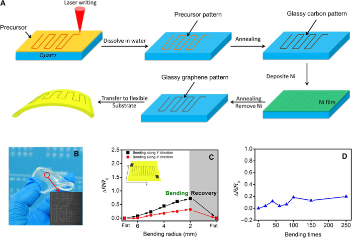
To further explore the potential applications of PAD-deposited glassy graphene, we performed laser direct writing for glassy graphene patterns/circuits. The polyethylenimine (PEI)–glucose precursor shows a thermal curing property. An infrared laser (1064 nm) is used to write a curing pattern on the precursor film, and the uncured part of the precursor could be easily removed by dissolving the film in water. As a result, a circuit pattern is readily obtained after the laser writing and rinsing process (Fig. 4A). Following the annealing process, the glassy graphene circuits can be transferred from the quartz substrate to any substrate afterward, for example, a flexible substrate (Fig. 4B). It should be noted that the sheer resistance increases from 10 to 15% after transfer (fig. S2). In addition, the electromechanical properties of the glassy graphene meander line pattern on flexible substrates were evaluated by bending experiments. In Fig. 4C, the sheet resistance increases with increasing bending radius, and the film recovers its original conductivity after the strain is released. The strain-dependent resistance vibration (ΔR/R0) of the meander line shows an anisotropic character; ΔR/R0 upon bending in the direction perpendicular to the meander line axis (Y direction) is more sensitive than that in the direction parallel to the meander line axis (X direction). After repeated bending or twisting (250 times), the glassy graphene film’s resistance does not show any obvious variation (Fig. 4D). Thus, one can conclude that the glassy graphene thin film is as reliable and flexible as graphene (10, 12). In addition, a complete graphene field-effect transistor was produced to demonstrate its potential application for graphene-based circuits (fig. S3) (28).

(A) Laser direct writing of glassy graphene circuits. (B) Image of glassy graphene circuits on a flexible substrate. The inset shows the as-written circuits. (C) Variation in resistance of a glassy graphene film on a polydimethylsiloxane (PDMS) substrate at different bending radii. (D) The variation in resistance after repeated bending up to 250 times.
DISCUSSION
The microstructure of the glassy graphene thin film is in an intermediate state between glassy carbon and graphene and shows high crystallinity with a twisted/bent lattice. By inheriting both the properties of glassy carbon and graphene, the glassy graphene thin film exhibits excellent conductivity, transmittance, and flexibility, as well as outstanding mechanical and chemical stability. The aqueous polymer molecular precursor solution not only enables the formation of glassy graphene thin films at the wafer scale with less than 1 nm roughness but also allows for the easy laser direct writing of complicated circuits on any substrate. The ultra-smooth surface of glassy graphene (0.7 nm) satisfies the industrial requirement of surface roughness (less than 1 nm) in current integrated devices. As a result, the developed flexible and transparent circuits based on conductive glassy graphene show great promise for future electronics applications.
The distinct microstructure of the glassy graphene might lead to different electronic band structures. The imperfect and distorted lattice reduces the conductivity and transparency of glassy graphene as compared to perfect graphene (Fig. 3, B and C). Nevertheless, the bent/twisted lattice implies the existence of intrinsic strain in glassy graphene, and this is expected to generate pseudomagnetic fields and induce valley polarization as found in graphene (29, 30). The strain effect in glassy graphene is an interesting topic for further study. It could pave the way for new applications in spin electronic devices.
MATERIALS AND METHODS
For a typical procedure, a homogeneous aqueous solution of glucose and PEI was spin-coated on clean quartz substrates and then annealed in an Ar/H2 atmosphere. The key to depositing a high-quality thin film is the inclusion of PEI, which increases the viscidity of the precursor and assists in the homogeneous polymerization of glucose molecular layers. As shown by the thermal weight analysis (fig. S4), pure glucose began to dehydrate at 250°C and lost 70% of its mass at 350°C, whereas PEI began to decompose at 310°C and lost 50% of its weight at 350°C. Therefore, PEI restrained aggregation during the initial dehydration stage of glucose. Without polymer assistance, the resultant film was porous and discontinuous (fig. S5).
Preparation of precursor and the annealing process
Glucose (1 g) (99.5%; Aldrich) and PEI (0.5 g) (molecular weight, ~25,000, branched; Aldrich) were dissolved in 5 ml of deionized water and stirred vigorously at room temperature for 12 hours. The quantity of glucose could be tuned from 1 to 0.2 g to adjust the glassy carbon film thickness. The precursor was then spin-coated onto quartz substrates at 8000 revolutions per minute for 30 s. Then, the precursor films were annealed gradually to 1000°C (2°C/min) in an Ar/H2 (10/1) atmosphere. Thereafter, the films were cooled down to room temperature after annealing at 1000°C for 5 min. To further enhance the crystallinity of the as-obtained glassy carbon film, the Ni thin film was evaporated on top of the film. Glassy graphene was obtained through reannealing at 850°C, and graphene was obtained through reannealing at 1000°C. The residual Ni was removed through etching in 1 M FeCl3 solution.
Characterization
The surface of the glassy graphene thin films was characterized by an atomic force microscope (Asylum Research MFP-3D-BIO), a scanning electron microscope (Hitachi SU8010), and an optical microscope (Shanghai Changfang CMM-55E). The thicknesses of the films were tested by scanning the step between the film and the substrate using an atomic force microscope. The microstructures of glassy graphene thin films were characterized using HRTEM (FEI Tecnai G20) and micro-Raman spectroscopy (RAMAN, Renishaw, inVia Reflex). The ultraviolet-visible absorption spectrum is recorded on a UV-2501PC spectrometer (Shimadzu). The sheet resistances of glassy graphene thin films were probed using a four-point probe resistivity measurement system (Guangzhou 4-Probes Tech, RTS-9).
Transfer process from quartz substrates to PDMS substrates
PDMS (Sylgard 184, Dow Corning) was prepared by mixing a curing agent and an elastomeric base at a 1:10 weight ratio. The freshly mixed PDMS was sprayed onto a glassy graphene/quartz substrate and cured at 70°C for 12 hours. Afterward, the quartz substrate was removed by immersing it in NaOH solution (1 M) for 48 hours.
Laser direct writing conditions
A laser direct writing machine was applied to carry out the pattern writing process (FT-LDW-IR20, Suzhou FTI Co. Ltd.). The wavelength, power, frequency, and scan speed of the pulsed laser are 1064 nm, 3.5 W, 60 kHz, and 120 mm/s, respectively.
Acknowledgments
Funding: We gratefully acknowledge support from the “973 Program—the National Basic Research Program of China” Special Funds for the Chief Young Scientist (2015CB358600), the Excellent Young Scholar Fund from the National Natural Science Foundation of China (21422103), the National Natural Science Foundation of China (21601130 and 21671141), the Jiangsu Fund for Distinguished Young Scientist (BK20140010), the Priority Academic Program Development of Jiangsu Higher Education Institutions, and the Jiangsu Scientific and Technological Innovation Team (2013). The TEM work at Texas A&M University was supported by the U.S. NSF (DMR-1401266). Author contributions: X.D., J.W., and Z.Q. carried out the precursor preparation and film deposition; Y.C. carried out Raman measurements and assisted in the annealing process; J.J. and H.W. carried out TEM measurements; Q.Y. carried out SEM measurements; X.D. carried out AFM measurements; X.D., J.W., Z.Q., and G.Z. assisted in the data analysis; G.Z. and H.W. supervised the project; G.Z., H.L., M.H.R., H.W., and X.D. co-drafted the paper with contributions from the rest of the authors. Competing interests: The authors declare that they have no competing interests. Data and materials availability: All data needed to evaluate the conclusions in the paper are present in the paper and/or the Supplementary Materials. Additional data related to this paper may be requested from the authors.
SUPPLEMENTARY MATERIALS
Supplementary material for this article is available at http://advances.sciencemag.org/cgi/content/full/2/11/e1601574/DC1
fig. S1. HRTEM images of glassy graphene.
fig. S2. Resistance and conductivity of glassy graphene thin films after transfer.
fig. S3. Structure and property of the glassy graphene field-effect transistor.
fig. S4. Time gravity analysis of the glucose-PEI mixture compared to that of PEI and glucose.
fig. S5. PEI-assisted film growth.
REFERENCES AND NOTES
Articles from Science Advances are provided here courtesy of American Association for the Advancement of Science
Full text links
Read article at publisher's site: https://doi.org/10.1126/sciadv.1601574
Read article for free, from open access legal sources, via Unpaywall:
https://advances.sciencemag.org/content/advances/2/11/e1601574.full.pdf
Citations & impact
Impact metrics
Citations of article over time
Alternative metrics
Smart citations by scite.ai
Explore citation contexts and check if this article has been
supported or disputed.
https://scite.ai/reports/10.1126/sciadv.1601574
Article citations
The Progress on Magnetic Material Thin Films Prepared Using Polymer-Assisted Deposition.
Molecules, 28(13):5004, 26 Jun 2023
Cited by: 2 articles | PMID: 37446666 | PMCID: PMC10343622
Review Free full text in Europe PMC
Different Roles of Surface Chemistry and Roughness of Laser-Induced Graphene: Implications for Tunable Wettability.
ACS Appl Nano Mater, 6(18):16201-16211, 10 Jul 2023
Cited by: 3 articles | PMID: 37772265 | PMCID: PMC10526650
SU-8 cantilever with integrated pyrolyzed glass-like carbon piezoresistor.
Microsyst Nanoeng, 8:22, 10 Feb 2022
Cited by: 3 articles | PMID: 35223080 | PMCID: PMC8831616
Three-Dimensional (3D) Laser-Induced Graphene: Structure, Properties, and Application to Chemical Sensing.
ACS Appl Mater Interfaces, 13(26):30245-30260, 24 Jun 2021
Cited by: 39 articles | PMID: 34167302 | PMCID: PMC8289247
Review Free full text in Europe PMC
Recent Studies on Dispersion of Graphene-Polymer Composites.
Polymers (Basel), 13(14):2375, 20 Jul 2021
Cited by: 5 articles | PMID: 34301133 | PMCID: PMC8309616
Review Free full text in Europe PMC
Go to all (13) article citations
Data
Data behind the article
This data has been text mined from the article, or deposited into data resources.
BioStudies: supplemental material and supporting data
Similar Articles
To arrive at the top five similar articles we use a word-weighted algorithm to compare words from the Title and Abstract of each citation.
Vacuum-Assisted Low-Temperature Synthesis of Reduced Graphene Oxide Thin-Film Electrodes for High-Performance Transparent and Flexible All-Solid-State Supercapacitors.
ACS Appl Mater Interfaces, 10(13):11008-11017, 21 Mar 2018
Cited by: 9 articles | PMID: 29528215
Large scale, highly conductive and patterned transparent films of silver nanowires on arbitrary substrates and their application in touch screens.
Nanotechnology, 22(24):245201, 20 Apr 2011
Cited by: 84 articles | PMID: 21508460
Large-scale plasma patterning of transparent graphene electrode on flexible substrates.
Langmuir, 31(9):2914-2921, 25 Feb 2015
Cited by: 2 articles | PMID: 25692852
A review of fabrication and applications of carbon nanotube film-based flexible electronics.
Nanoscale, 5(5):1727-1752, 05 Feb 2013
Cited by: 212 articles | PMID: 23381727
Review
Funding
Funders who supported this work.
Engineering and Physical Sciences Research Council (1)
Grant ID: EP/K029118/1


